FOR COMPONENT BUYERS
Semiconductors & optical modules
Build your bill of materials around wavelength, optical power, package, thermal design and application constraints.
Browse the product platform
PHOTONIC SEMICONDUCTORS · LIGHT ENGINES · OEM/ODM
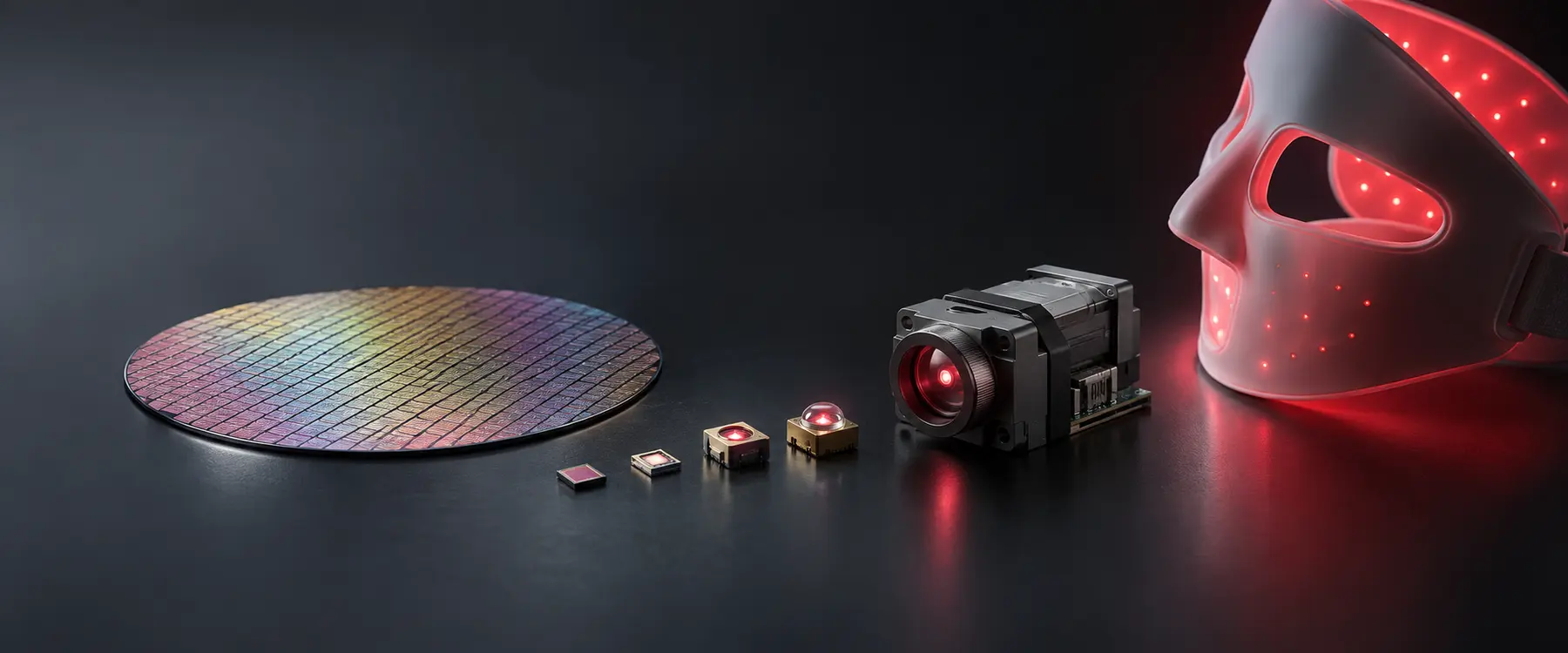
Custom emitters, optical modules and engineering support for sensing, medical beauty and intelligent devices.
B2B PATHWAYS
Two buyer journeys, one photonics platform. Component teams can source emitters and modules; device brands can move into a managed OEM/ODM program.
FOR COMPONENT BUYERS
Build your bill of materials around wavelength, optical power, package, thermal design and application constraints.
Browse the product platformFOR DEVICE BRANDS
Develop light-based beauty and personal-care devices with optical, thermal, industrialization and manufacturing support.
Plan an OEM/ODM projectPRODUCT PLATFORM
The catalog is organized by buyer decision—not internal technology labels—so engineering teams can move from emitter selection to a qualified module request.
Open the full product centerRed and yellow wavelength families for indicators, displays, sensing and light-based applications.
Blue and green wavelength families for indicators, specialty lighting and optical systems.
Infrared emitters for sensing, illumination, machine vision and device integration.
Vertical-cavity laser sources for proximity, time-of-flight, structured illumination and custom modules.
Multi-emitter layouts engineered around coverage, thermal path and assembly requirements.
Integrated source, optics and drive coordination for compact sensing or illumination assemblies.
Custom light-source assemblies for wearable, handheld and professional beauty-device concepts.
Application-specific assemblies combining emitters, optics, electronics and mechanical interfaces.
APPLICATIONS
The site keeps chips and medical beauty together because the value chain is continuous. Each application has its own technical entry point, evidence requirements and commercial workflow.
Emitter selection, illumination geometry and compact module integration.
Light engines and device programs for photobiomodulation and beauty concepts.
Compact visible and infrared sources for intelligent device features.
Wavelength-specific platforms for industrial and application-defined lighting.
CAPABILITY ENVIRONMENTS
These original campaign visualizations communicate the operating environments relevant to a photonics supplier. They are not documentary photographs of a specific CECL site, team or exhibition and will be replaced as verified photography becomes available.

A brand visualization for the scale and operating environment expected by global B2B programs.
Original brand visualization
Wafer handling, die inspection and precision manufacturing workflow visualization.
Original brand visualization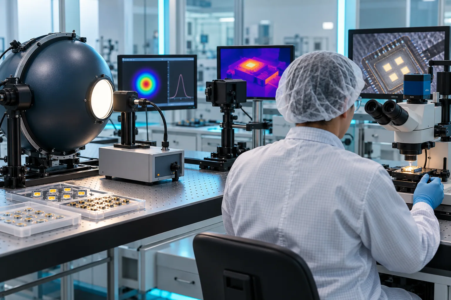
A measurement environment covering optical power, beam, thermal and microscopic inspection.
Original brand visualization
Inspection, anti-static handling, moisture protection, packing and dispatch workflow.
Original brand visualization
Application, optics, electronics, industrialization and export requirements reviewed together.
Original brand visualization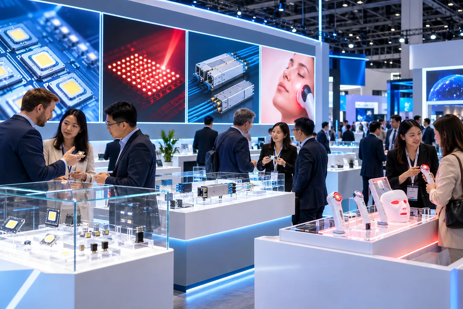
A campaign visualization of component, module and beauty-device sourcing conversations.
Original brand visualizationMEDICAL BEAUTY & PERSONAL CARE
A separate device pathway lets brand owners discuss form factor, optical uniformity, heat, controls, production targets and market documentation without navigating a component catalog.
Example program directions
Uniform light delivery, comfort, controls and manufacturability.
Wearable optical architecture, thermal comfort and usage design.
Portable form factor, interchangeable optics, charging and accessory planning.
Coverage, serviceability, control zones and production planning.
DEVICE PLATFORM CONCEPTS
These original concept visuals show how CECL emitter and light-engine capabilities may translate into branded device programs. Final appearance, optical parameters, claims and compliance route are defined project by project.
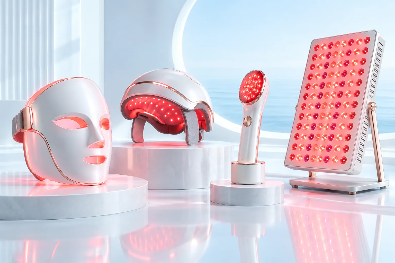
Multi-wavelength layouts shaped around facial coverage, eye protection, fit and thermal comfort.
Configurable by projectDense optical arrays, wearable geometry, session control and heat-management planning.
Configurable by projectCompact emitters and optics for targeted coverage, charging, controls and accessory ecosystems.
Configurable by projectZoned illumination, serviceable modules and scalable mechanical architecture for professional environments.
Configurable by projectOEM / ODM WORKFLOW
Each gate produces a concrete decision: requirements, optical architecture, prototype, validation package and manufacturing release.
Application, market, volume stage and commercial target.
Emitter, optics, electronics, thermal and mechanical concept.
Evaluation unit or device sample for agreed test objectives.
Performance, reliability and market-document review plan.
Process confirmation, inspection criteria and limited build.
Approved specification, change control and supply planning.
PHOTONICS KNOWLEDGE
Original industry articles connect component selection, device engineering and market documentation. They are written for brand owners, distributors and engineering teams—not for keyword stuffing.
01
A practical framework for turning a desired use case into emitter, optical and validation requirements.
Read article02
Why package, optics, drive, heat and mechanical integration should be reviewed as one system.
Read article03
Separate component test reports, device verification and destination-market evidence before placing an order.
Read article04
Compare optical power, pulse conditions, beam, efficiency and thermal limits before requesting samples.
Read article05
A procurement checklist for bins, output, voltage, test conditions and change control.
Read article06
Settle optics, thermal comfort, controls, validation and manufacturing inputs before tooling.
Read articleTRUST & DOCUMENTATION
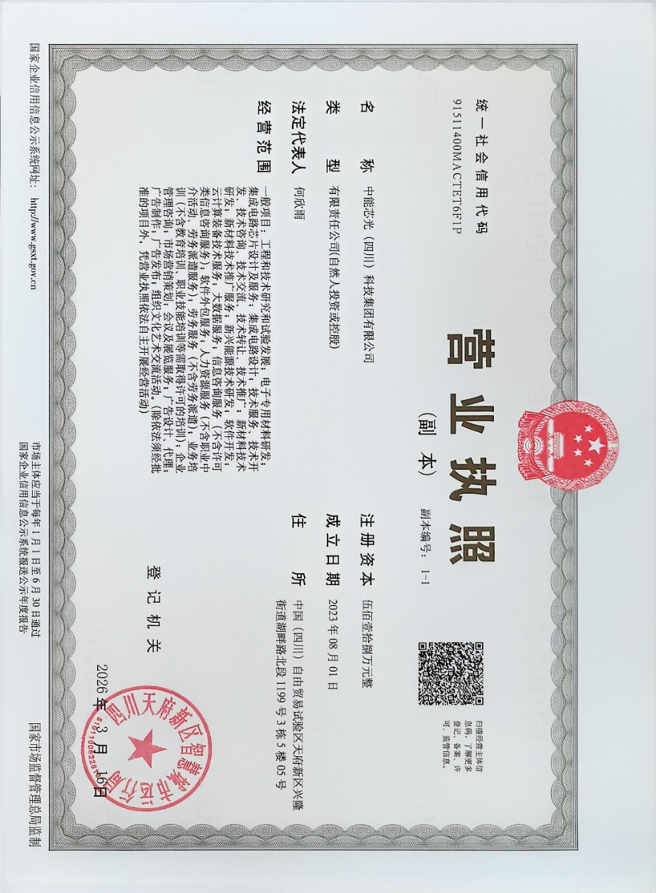
This site avoids unverified performance and certification claims. Buyers can review supplied business records, SGS reports and product catalogs, then request the documentation set for the exact part and target market.
Open document centerDatasheet, drawing, operating limits and handling information for the selected model.
Inspection approach, reliability items and traceability scope available by product program.
Applicable declarations, reports or planning inputs reviewed against device and destination market.
VERIFICATION LIBRARY
Original files supplied for this website are grouped by purpose. Test results apply to the submitted LED chip sample and the scope stated in each report; they are not blanket certification for every product or finished device.
SGS · CANEC25028451601 / 1602
Conclusion: Pass
SGS · CANEC25028451603
251 Candidate List SVHC and 4 potential SVHC: ≤ 0.1% (w/w)
SGS · CANEC25028451605 / 1606
F, Cl, Br and I reported ND at the stated method detection limits
SGS · CANEC25028451607 / 1608
Conclusion: Pass
Proximity, medical beauty, obstacle avoidance, liquid level and industrial sensing applications.
Visible red, orange, yellow and yellow-green families, plus selected infrared series.
Lighting, display, backlight, automotive and visible blue/green product families.
BUYER FAQ
Yes. Component and module inquiries follow their own sample, specification and quotation path.
Yes. That continuity is the main reason the two businesses share one B2B website.
Certification applicability depends on the final device, claims and destination market. Evidence should be reviewed for the exact configuration.
Application, preferred wavelength or effect, physical constraints, estimated volume stage, target market and timeline are enough to begin.
START A PROJECT
Share what is already known—application, wavelength, package or device concept, volume stage and destination market. Missing details can be resolved during engineering review.